
Laboratories
Investigating optical properties of 2D materials
Raman spectrometer based on confocal microscope
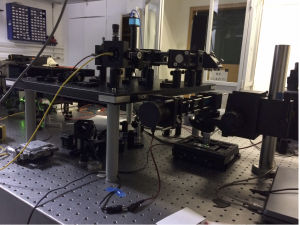
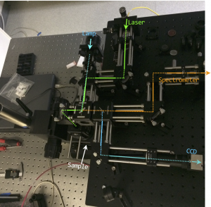
Optical setup based on confocal microscope in backscattered configuration serves for absorption (contrast reflectivity), photoluminescence and Raman spectra measurements. Excitation laser power is maintained sufficiently low to avoid damage to the sample. At the moment, three excitation laser lines are provided: 488, 532 and 630 nm. A home-made confocal microscope based on cage system design is equipped with an appropriate set of filters, dichroic mirrors, polarization plates and objective lens. Collected backscattered light is guided through an optical fiber with a 50 μm core diameter, which acts as a confocal detection pinhole to a 30 cm long spectrograph equipped with a cooled electron multiplying charge coupled device – EM CCD that increases sensitivity for challenging samples with low signal levels. Triple Raman spectrometer with 300, 600 and 1800 grooves/mm diffraction gratings is used to collect the absorption, photoluminescence and Raman spectra, respectively. Recently, low-energy Raman modes can be measured since the experimental setup is upgraded with the set of volume Bragg filters that serve as optical filters with extremely narrow linewidths. Polarization-resolved measurements are achieved by of various optically active elements (quarter- and half-waveplates and polarizers) in both excitation and detection branch.
Equipped with xy-translator stages, confocal setup provides both a sequential sample movement and spectrum data acquisition from the defined sample area with sub-micron resolution. In this way spatial maps of the sample are created. A software platform is developed to deliver an intuitive and user-friendly interface for data acquisition, data processing, data analysis and display. Confocal spectral imaging will be used to obtain the local spectra at each scanning pixel position.
Second harmonic microscopy setup
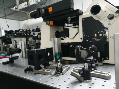 New experimental setup is based on a pulsed titanium-sapphire oscillator with 100 fs pulses and a repetition rate of 80 MHz. The laser beam, modulated by mechanical chopper is focused onto the sample using a microscope objective. The second harmonic is detected in backscattering geometry by an avalanche photodiode (APD). The incident near-infrared laser beam and the visible second harmonic response are separated employing a cold mirror, which only reflects short wavelengths, therefore SHG signal. Subsequently, the scattered laser beam is further suppressed by several short-pass filters. Positioning of the sample using an optical microscope image is realized with a halogen lamp, a camera and a motorized XY translation stage. Polarization measurements are achieved by tuning the polarization of the incident by a rotatable polarizer instead of a manual sample rotation. For spatial mapping of the sample, xy-translator stages are employed.
Synthesis of 2D materials
A small-scale CVD setup can operate under atmospheric pressure (precursors in the flow of Ar gas) or low vacuum. The advantages of the setup are in its small size and high quality insulation enabling direct optical access with a view on the growth substrate, giving the in-situ control of the growth process. The small size makes it compatible with a fume hood or a glovebox. The small size also enables fast sample heating and cooling rates, something well beyond the performance of commercially available CVD furnaces and low expenditure and footprint. We have implemented several different ways of precursor delivery, like separate heaters for chalcogens or laser-assisted evaporation of metal precursor, which along with seeding promoters deposited at the substrate prior to growth give us wide phase space for controlling the growth parameters. This setup also provides us with real time-dynamics of the growth process, which will be especially of use in controlling the growth dynamics in multistep growth procedures. Recently, we have developed a transfer technique for successful deposition of 2D crystals (monolayers, homo- and heterolayers) on arbitrary substrate.
Atomic Force Microscopy (AFM)
The NanoWizardULTRA Speed 2 advanced AFM system combines fast scanning with high resolution at scan sizes: it reaches speed levels previously unattainable with traditional AFMs and combines true atomic resolution and fastest scanning with rates of 10 frames/sec. Real-time, in-situ experiments can be performed in combination with advanced optics. A broad range of modes and accessories makes the system highly flexible and upgradable.
It provides a range of new features:
- high-speed imaging of surface structures up to 8µm with outstanding resolution and stability
- easy imaging
- automated mapping of large sample areas
- revolutionary new workflow-based user interface
- software for perfect integration and data correlation with advanced fluorescence microscopy platforms
- controller for high-speed signal processing and lowest noise levels